Purpose
The RT6255B is a synchronous step-down converter with Advanced Constant On-Time (ACOT™) mode control. with the input voltage range from 4.5V to 18V and provides 5A output current. This document explains the function and use of the RT6255B evaluation board (EVB), and provides information to enable operation, modification of the evaluation board and circuit to suit individual requirements.
Introduction
General Product Information
The RT6255B is a high-efficiency, synchronous stepdown DC-DC converter that can deliver up to 5A output current from a 4.5V to 18V input supply. The RT6255B adopts Advanced Constant On-Time (ACOT™) control architecture to provide an ultrafast transient response with few external components and to operate in nearly constant switching frequency over line, load, and output voltage ranges.
The RT6255B features cycle-by-cycle current limit protection against short-circuit outputs, and soft-start function to prevent inrush current during start-up. It also includes input under-voltage lockout, output under-voltage protection, and over-temperature protection (thermal shutdown) to provide safe and smooth operation in all operating conditions.
Product Feature
- Input Supply Voltage Range : 4.5V to 18V
- Output Current : 5A
- Advanced Constant On-Time (ACOT™) Control for Ultrafast Transient Response
- Steady Switching Frequency : 500kHz
► Forced PWM Mode
- Optimized for Low-ESR Ceramic Output Capacitors
- Programmable Output Voltage : 0.6V to 5V
- Internal 45mΩ Switch and 23mΩ Synchronous Rectifier
- Cycle-by-Cycle Current Limit Protection
- Internal Soft-Start (Typ 1.5ms) or Externally
- Adjustable, Pre-biased Compatible Soft-Start (Only for Option with SS Pin)
- Power Good Indicator (90%) (Only for Option with PGOOD Pin)
- Output Under-Voltage Protection (UVP)
- Over-Temperature Protection (OTP)
- Input Under-Voltage Lockout (UVLO)
- Available in TSOT-23-8 (FC)Packages
Key Performance Summary Table
|
Key Features
|
Evaluation Board Number : PCB102_V1
|
|
Default Input Voltage
|
12V
|
|
Max Output Current
|
5A
|
|
Default Output Voltage
|
5V
|
|
Default Marking & Package Type
|
RT6255BHGJ8F, TSOT-23-8 (FC)
|
|
Operation Frequency
|
Steady 500kHz at all loads
|
Bench Test Setup Conditions
Headers Description and Placement
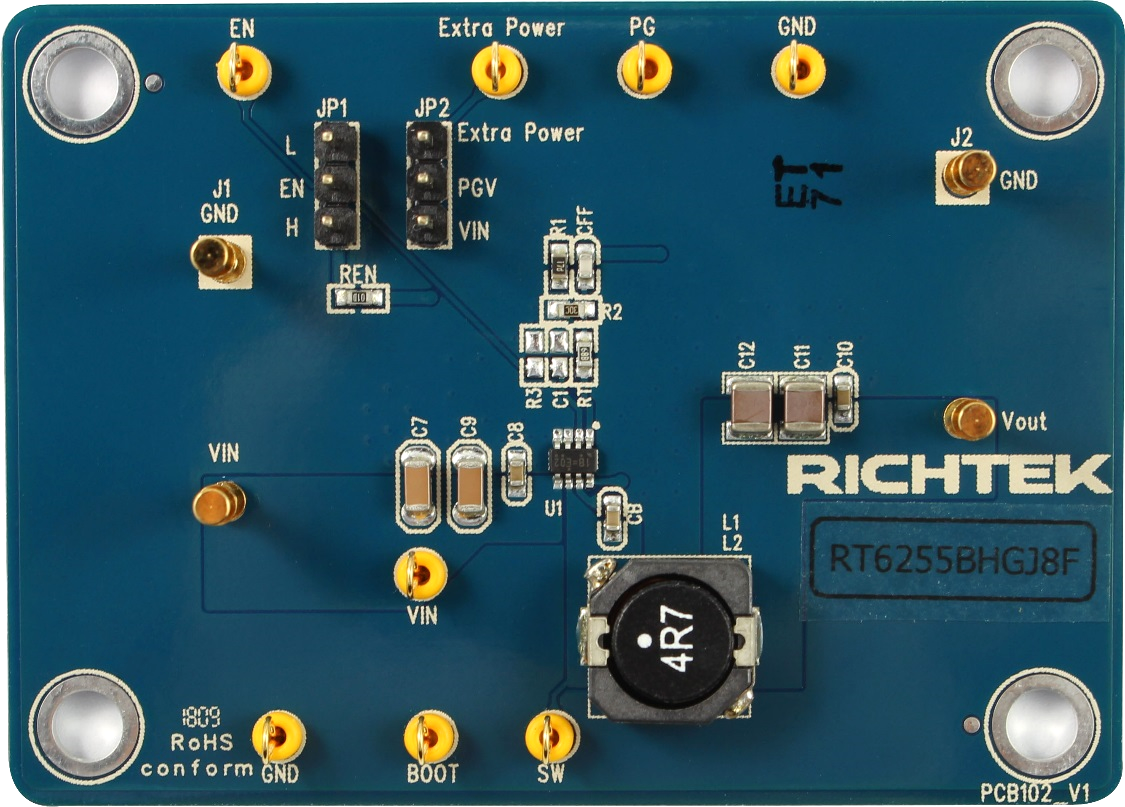
Carefully inspect all the components used in the EVB according to the following Bill of Materials table, and then make sure all the components are undamaged and correctly installed. If there is any missing or damaged component, which may occur during transportation, please contact our distributors or e-mail us at evb_service@richtek.com.
Test Points
The EVB is provided with the test points and pin names listed in the table below.
|
Test point/
Pin name
|
Signal
|
Comment (expected waveforms or voltage levels on test points)
|
|
VOUT
|
Output Voltage Test Point
|
This pin is used to sense output voltage.
|
|
VIN
|
Input voltage
|
Power input. Supplies the power switches of the device.
|
|
GND
|
Ground
|
This is the power return for the IC.
|
|
BOOT
|
Bootstrap
|
Bootstrap supply for high-side gate driver. Connect a 0.1µF ceramic capacitor from LX to BOOT to power the high-side switch.
|
|
SW
|
Switch Node Test Point
|
Connect the output LC filter from SW to the output load.
|
|
EN
|
Enable Control Input
|
Floating this pin or connecting this pin to logic high can enable the device and connecting this pin to GND can disable the device.
|
|
Extra Power
|
External Pull High Voltage
|
External power supply input for PGOOD pulls high power.
|
|
PG
|
Power Good Indicator
|
Power good indicator. Open-drain output when the output voltage is within 90% to 120% of regulation point.
|
Power-up & Measurement Procedure
1. Apply a 12V nominal input power supply (4.5V < VIN < 18V) to the VIN and GND terminals.
2. Set the jumper at JP1 to connect terminals 2 and 3, connecting EN to VIN through resistor REN, to enable
operation.
3. Verify the output voltage (approximately 5V) between VOUT and GND.
4. Connect an external load up to 5A to the VOUT and GND terminals and verify the output voltage and current.
Output Voltage Setting
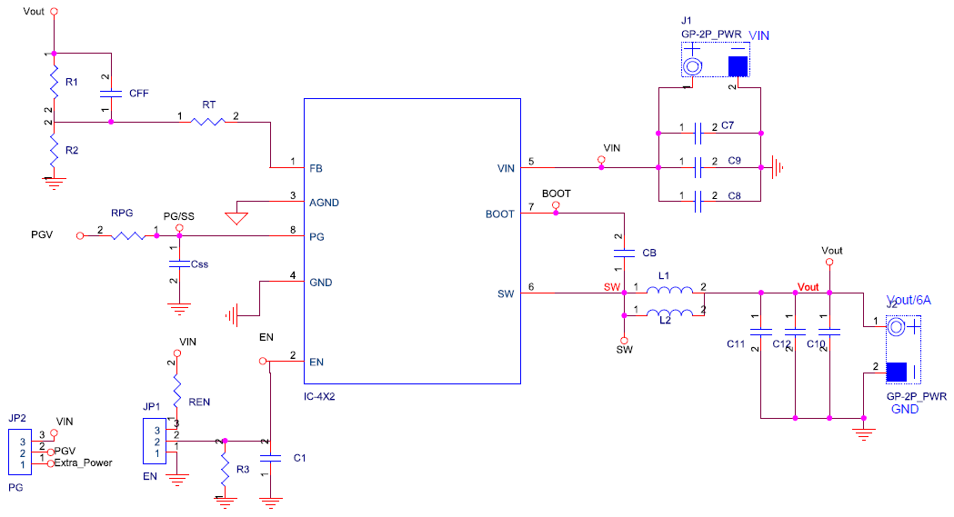
Set the output voltage with the resistive divider (R1, R2) between VOUT and GND with the midpoint connected to FB. The output is set by the following formula :
VOUT = VFB x (1 + R1 / R2)
Schematic, Bill of Materials & Board Layout
EVB Schematic Diagram
Bill of Materials
|
Reference
|
Qty
|
Part Number
|
Description
|
Package
|
Manufacturer
|
|
U1
|
1
|
RT6255BHGJ8F
|
DC-DC Converter
|
TSOT-23-8 (FC)
|
RICHTEK
|
|
C7, C9
|
2
|
C3216X5R1H106K160AB
|
10µF/50V/X5R/1206
|
C-1206
|
TDK
|
|
C8, C10, CB, CSS
|
4
|
GRM188R71H104KA93D
|
100nF/50V/X7R/0603
|
C-0603
|
MURATA
|
|
CFF
|
1
|
0603N470J500CT
|
47pF/50V/NPO/0603
|
C-0603
|
WALSIN
|
|
C11, C12
|
2
|
C3225X5R1E226M250AC
|
22µF/25V/X5R/1210
|
C-1210
|
TDK
|
|
L1
|
1
|
7447714047
|
4.7µH
|
L-10x10
|
Wurth Electronics
|
|
REN
|
1
|
WR06X1003FTL
|
100k
|
R-0603
|
WALSIN
|
|
R1
|
1
|
WR06X1473FTL
|
147k
|
R-0603
|
WALSIN
|
|
R2
|
1
|
WR06X2002FTL
|
20k
|
R-0603
|
WALSIN
|
|
RT
|
1
|
WR06X4991FTL
|
4.99k
|
R-0603
|
WALSIN
|
|
C1, L2, R3, RPG
|
4
|
|
NC
|
C-0603
|
|
PCB Layout
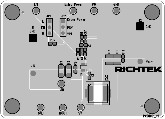
Top View (1st layer)

PCB Layout—Inner Side (2nd Layer)

PCB Layout—Inner Side (3rd Layer)
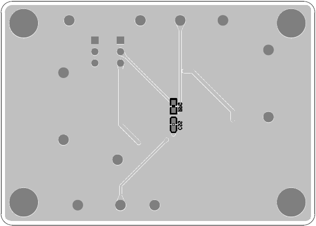
Bottom View (4th Layer)